- 您现在的位置:买卖IC网 > Sheet目录1992 > CYW150OXC (Silicon Laboratories Inc)IC CLOCK 440BX AGP 56SSOP
CYW150
...................... Document #: 38-07177 Rev. *B Page 11 of 14
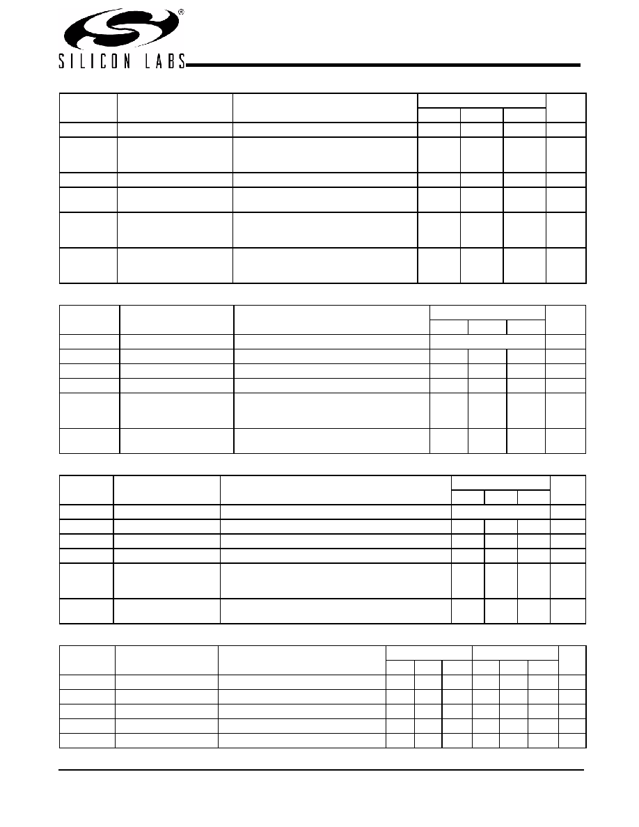
tD
Duty Cycle
Measured on rising and falling edge at 1.5V
45
55
%
tJC
Jitter, Cycle-to-Cycle
Measured on rising edge at 1.5V. Maximum
difference of cycle time between two
adjacent cycles.
250
ps
tSK
Output Skew
Measured on rising edge at 1.5V
500
ps
tO
CPU to PCI Clock Skew
Covers all CPU/PCI outputs. Measured on
rising edge at 1.5V. CPU leads PCI output.
1.5
4
ns
fST
Frequency Stabilization
from Power-up (cold start)
Assumes full supply voltage reached within
1 ms from power-up. Short cycles exist prior
to frequency stabilization.
3ms
Zo
AC Output Impedance
Average value during switching transition.
Used for determining series termination
value.
15
IOAPIC0 and IOAPIC_F Clock Outputs (Lump Capacitance Test Load = 20 pF)
Parameter
Description
Test Condition/Comments
CPU = 66.6/100 MHz
Unit
Min.
Typ.
Max.
f
Frequency, Actual
Frequency generated by crystal oscillator
14.31818
MHz
tR
Output Rise Edge Rate
Measured from 0.4V to 2.0V
1
4
V/ns
tF
Output Fall Edge Rate
Measured from 2.0V to 0.4V
1
4
V/ns
tD
Duty Cycle
Measured on rising and falling edge at 1.25V
45
55
%
fST
Frequency Stabilization
from Power-up (cold start)
Assumes full supply voltage reached within
1 ms from power-up. Short cycles exist prior to
frequency stabilization.
1.5
ms
Zo
AC Output Impedance
Average value during switching transition.
Used for determining series termination value.
15
REF0:1 Clock Outputs (Lump Capacitance Test Load = 20 pF)
Parameter
Description
Test Condition/Comments
CPU = 66.6/100 MHz
Unit
Min.
Typ.
Max.
f
Frequency, Actual
Frequency generated by crystal oscillator
14.318
MHz
tR
Output Rise Edge Rate
Measured from 0.4V to 2.4V
0.5
2
V/ns
tF
Output Fall Edge Rate
Measured from 2.4V to 0.4V
0.5
2
V/ns
tD
Duty Cycle
Measured on rising and falling edge at 1.5V
45
55
%
fST
Frequency Stabilization
from Power-up (cold
start)
Assumes full supply voltage reached within 1 ms from
power-up. Short cycles exist prior to frequency stabili-
zation.
3ms
Zo
AC Output Impedance
Average value during switching transition. Used for
determining series termination value.
25
SDRAM 0:15, _F Clock Outputs (Lump Capacitance Test Load = 30 pF)
Parameter
Description
Test Condition/Comments
CPU = 66.8 MHz
CPU = 100 MHz
Unit
Min.
Typ.
Max.
Min.
Typ.
Max.
t
P
Period
Measured on rising edge at 1.5V
15
15.5
10
10.5
ns
tH
High Time
Duration of clock cycle above 2.4V
5.2
3.0
ns
tL
Low Time
Duration of clock cycle below 0.4V
5.0
2.0
ns
tR
Output Rise Edge Rate Measured from 0.4V to 2.4V
1
4
1
4
V/ns
tF
Output Fall Edge Rate
Measured from 2.4V to 0.4V
1
4
1
4
V/ns
PCI Clock Outputs, PCI_F and PCI0:5 (Lump Capacitance Test Load = 30 pF) (continued)
Parameter
Description
Test Condition/Comments
CPU = 66.6/100 MHz
Unit
Min.
Typ.
Max.
发布紧急采购,3分钟左右您将得到回复。
相关PDF资料
CYW173SXC
IC CLK GEN TAPE DRV 4CH 16SOIC
CYW305OXC
IC CLOCK W305 SOLANO 56SSOP
DAC5674IPHPG4
IC DAC 14BIT 400MSPS 48-HTQFP
DAC7621EBG4
IC SNGL 12BIT PARALLEL D/A 20SSO
DAC7801KPG4
IC DUAL 12BIT CMOS DAC 24-DIP
DAC8043AESZ
IC DAC 12BIT MULT SRL INP 8SOIC
DAC8043GP
IC DAC 12BIT MULTIPLY CMOS 8-DIP
DAC8221GP
IC DAC 12BIT DUAL W/BUFF 24-DIP
相关代理商/技术参数
CYW150OXCT
功能描述:时钟发生器及支持产品 Legacy-440BX AGP Refer to W150 DS RoHS:否 制造商:Silicon Labs 类型:Clock Generators 最大输入频率:14.318 MHz 最大输出频率:166 MHz 输出端数量:16 占空比 - 最大:55 % 工作电源电压:3.3 V 工作电源电流:1 mA 最大工作温度:+ 85 C 安装风格:SMD/SMT 封装 / 箱体:QFN-56
CYW152-12G
制造商:Rochester Electronics LLC 功能描述:- Bulk
CYW15G0101DXB
制造商:CYPRESS 制造商全称:Cypress Semiconductor 功能描述:Single-channel HOTLink II⑩ Transceiver
CYW15G0101DXB-BBC
功能描述:电信线路管理 IC Sngl Ch XCVR COM RoHS:否 制造商:STMicroelectronics 产品:PHY 接口类型:UART 电源电压-最大:18 V 电源电压-最小:8 V 电源电流:30 mA 最大工作温度:+ 85 C 最小工作温度:- 40 C 安装风格:SMD/SMT 封装 / 箱体:VFQFPN-48 封装:Tray
CYW15G0101DXB-BBI
功能描述:电信线路管理 IC Sngl Ch XCVR IND RoHS:否 制造商:STMicroelectronics 产品:PHY 接口类型:UART 电源电压-最大:18 V 电源电压-最小:8 V 电源电流:30 mA 最大工作温度:+ 85 C 最小工作温度:- 40 C 安装风格:SMD/SMT 封装 / 箱体:VFQFPN-48 封装:Tray
CYW15G0101DXB-BBXC
制造商:CYPRESS 制造商全称:Cypress Semiconductor 功能描述:Single-channel HOTLink II⑩ Transceiver
CYW15G0101DXB-BBXI
功能描述:电信线路管理 IC HOTLink II 1.5Gbps Single Channel RoHS:否 制造商:STMicroelectronics 产品:PHY 接口类型:UART 电源电压-最大:18 V 电源电压-最小:8 V 电源电流:30 mA 最大工作温度:+ 85 C 最小工作温度:- 40 C 安装风格:SMD/SMT 封装 / 箱体:VFQFPN-48 封装:Tray
CYW15G0201DXB
制造商:CYPRESS 制造商全称:Cypress Semiconductor 功能描述:Dual-channel HOTLink II⑩ Transceiver